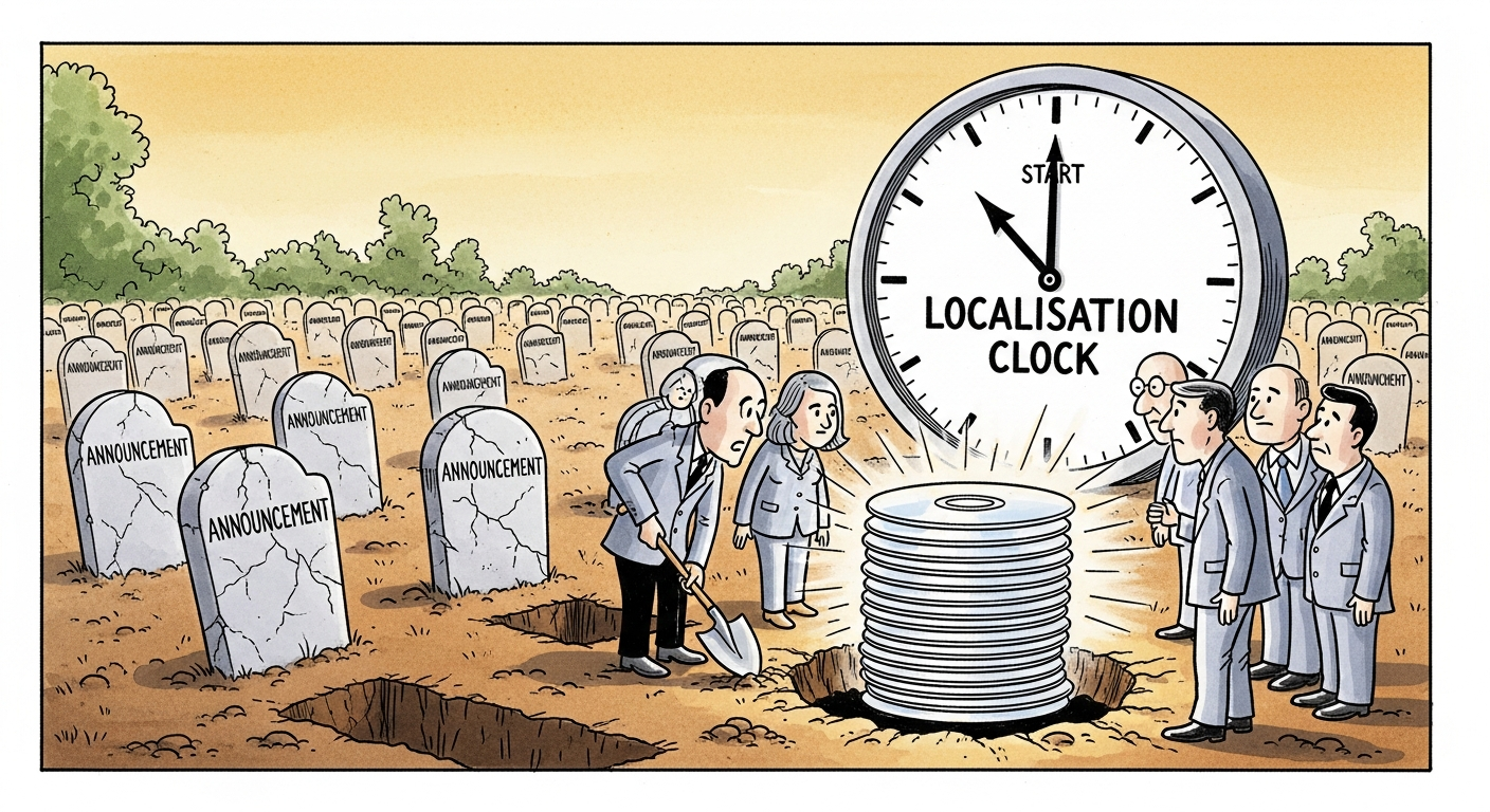
Countries don't remember test lots. India will remember this one: 25 wafers, 28 nanometres, within tolerance — the electrical results that turn a construction site into a factory and a fifty-year policy graveyard into a prehistory.
The contents are deliberately humble: power-management ICs and display drivers, the mature-node workhorses every Indian assembly line currently imports in entirety. First customers: two automotive-electronics suppliers and the consortium's own packaging plant at Sanand. The value chain the PLI built from the final screw backward just reached the die.
The speed is the anomaly: ground to wafers in twenty-six months, clean-room certified in nineteen — the Japan framework's equipment financing closing the tool-installation gap that killed every previous attempt at exactly this stage.
The honest asterisk: 400-plus process tools, zero Indian — yet. The localisation schedule contracts specialty gases and wet chemicals to Indian plants from next year; the first India-designed, Dholera-fabbed chips tape out this quarter.
One mature-node fab is not semiconductor power. It is the end of computing on silicon no Indian facility could print. The next lot is already in the line — and on our tech desk.