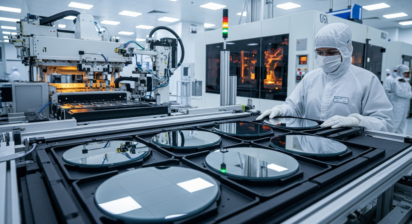
The Dholera fab's first risk-production lot — 25 wafers on the 28-nanometre process — returned electrical test results within tolerance this week, the facility's operating consortium confirmed: the milestone at which a semiconductor plant stops being a construction project and starts being a factory. Commercial risk production begins in the autumn; qualified volume output remains scheduled for mid-2027.
The lot's contents are deliberately unglamorous: power-management ICs and display drivers, the mature-node workhorses whose demand India's electronics assembly industry currently imports in entirety. The fab's first three customers are the anchor logic: two Indian automotive-electronics suppliers and the consortium's own OSAT facility, whose packaging lines in Sanand reach qualification in parallel.
The timeline behind the milestone bears recording because the country's semiconductor history is a graveyard of announcements. Ground broke twenty-six months ago; the clean-room certified in nineteen; the Japan framework's equipment-financing tranche — the corridor money the war quarter accelerated — closed the tool-installation gap that stalled every previous Indian fab attempt at the same stage. The project's engineers describe the achievement in supply-chain terms: 400-plus process tools, 60 vendors, zero of them Indian — yet.
That 'yet' is the policy's second act. The fab's localisation schedule contracts specialty-gas and wet-chemical supply to Indian plants from next year; the design-linked incentive's first chips — designed in Bengaluru, to be fabbed in Dholera — tape out this quarter.
A single mature-node fab does not make India a semiconductor power; Taiwan runs dozens at nodes a decade ahead. What the test lot ends is the prehistory: the era in which every Indian device, from missile to metro card, computed on silicon no Indian facility could print. The next lot is already in the line.