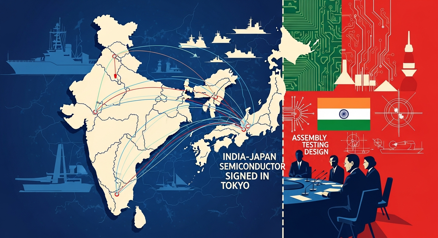
India and Japan signed a ¥2.1 trillion (approximately ₹1.2 lakh crore) semiconductor corridor framework in Tokyo on Friday, the concluding act of the economic forum both prime ministers have attended twice since May and the largest bilateral technology agreement in either country's record.
The framework's architecture is deliberate: Japan brings what India lacks — fabrication equipment, specialty chemicals, wafer-grade silicon — while India supplies what Japan's demographics no longer can: engineering headcount, assembly-test-packaging scale, and a domestic market growing at the fastest rate of any major economy.
Three anchor investments are named. A joint 40-nanometre analog fab at Dholera with a Japanese consortium holding 49 percent. An expansion of the Jagiroad ATMP cluster in Assam, already under construction, to triple capacity. And a power-electronics design centre in Kochi focused on the silicon-carbide devices that electric rail and grid storage demand.
The unstated architecture matters as much: every node in the corridor is a de-risking play against a Taiwan contingency both capitals now plan around openly. The framework includes a supply-assurance annexe — priority allocation to each other's markets during 'supply-chain emergencies' — the first such clause Japan has signed with any country.
Execution risk remains India's to carry. The corridor's first test is prosaic and near: Dholera's consortium needs 1,100 process engineers on site by March. The talent pipeline, not the capital, is the binding constraint — a fact the framework acknowledges by funding twelve fab-focused M.Tech programmes in its first tranche.